The Fusion 360 Signal Integrity Extension, powered by Ansys, unlocks additional PCB/electronics signal integrity tools and capabilities inside Fusion 360, allowing you to run electromagnetic analysis on critical signals within your PCB. Let’s walk you through how to get started.
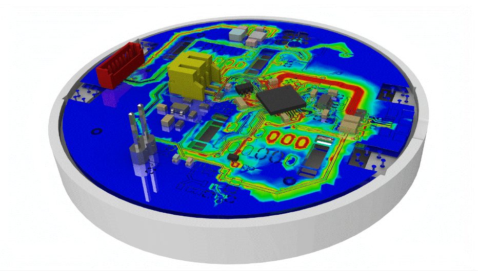
Before getting started, let us look at what we’re providing with the Fusion 360 Signal Integrity Extension, powered by Ansys. Figure 1 is a visualization of how a USB signal at about 500 megahertz travels. The Signal Integrity extension facilitates your ability to observe how impedance changes in real-time. The extension shows where your signal traces have impedance discontinuities and time delays, allowing you to troubleshoot your circuitry.
Let’s go over some simple concepts that will give more context on the use of the Signal Integrity Extension.
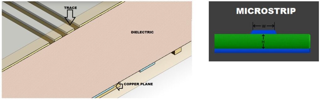
When working with signal integrity and high-speed signals, one of the critical points besides the specific impedance is having it be constant. If you have a constant cross-section, you have a continuous impedance near the trace of interest. If anything changes, such as the separation between polygons to the trace, if you have a gap or any change in that geometry will lead to a change in impedance. That takes us to the next point.
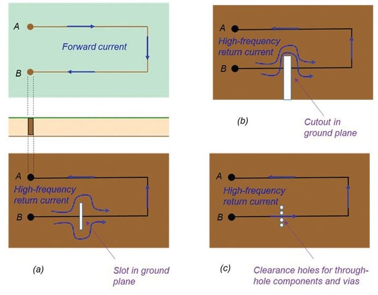
Current will always follow the path of least impedance. That path is the one that closely follows the forward current. There is the signal path, and you have a return path; since we all know that electricity flows and loops, our goal is to have both follow the same path to maintain constant impedance. In Figure 3, the image on the top left has no gaps in the return plane; therefore, it can follow the forward current. That is going to be the path of the least impedance.
Observe the other case scenarios (Figure 3. A, B, and C); any breaks in polygon fill will cause the return current to go around the plane, changing the impedance. Anywhere you have a cut in the plane, you will notice that the impedance will change because the return current must flow around that gap.
With these two very simple and straightforward ideas in mind, let’s learn how the Signal Integrity Extension works.
How does the Signal Integrity Extension work?

With the Fusion 360 Signal Integrity Extension active, you will notice the icon in the simulation tab (Figure 4). The Signal Integrity Extension conveniently appears as a panel in your PCB workspace.
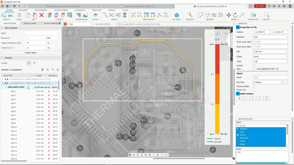
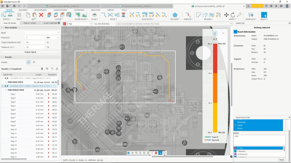
Select the signal you want to analyze, and its name will be automatically populated in the signal field. We have selected “D_P,” one of the USB’s differential pairs of interest whose impedance you want to analyze. You may also specify either a target impedance or not. If you don’t assign a target, it will show you how the impedance changes along the entire length of the trace. If you specify a tolerance, as observed in our video, the results will show you how it deviates from that target impedance. After analyzing the selected signal, the results show how far the trace deviates from the intended target at the ends.
We have a range of about 66 ohms at the minimum and a maximum of about 86 ohms. This confirms that we are way out of our intended target. Notice how the colors indicate what areas are off target. The darker the color, the stronger the red, and the more the signal deviated from the intended target. Every single segment has been simulated. Specific segments are more greatly deviated compared to others. From this analysis, we can determine we have two significant problems: a) We’re way out of the intended target impedance and b) we also have an inconsistent impedance profile.
Notice that near the ends there are areas where we have significant deviations. This is due to the separation that is changing between the differential pairs. At the same time, we also have areas where the polygon is broken. And because of that, there is no polygon fill in those areas, causing the impedance to change.
Additionally, you can simulate multiple signals at the same time. In the next figure (Figure 4), we simulate the D_N signal, and the Signal Integrity extension keeps track of both. Analyzing a second signal will NOT erase our initial results. This is beneficial since it allows us to compare results between each differential pair and see the relationship between multiple traces. It keeps the history of your traces and any analysis you do while using the extension within the session.
Creating space for the polygon

There are many ways to address signal integrity in your design. We will show the first fix to improving impedance – which is to make impedance constant. In this example (Figure 5), we have a lot of deviations. Notice that the lines have several colors on the segments; this means there are too many variations in our trace, and what we need is to accomplish one uniform color. Because this design was provided to us fully routed, we do not want to make too many changes. Instead, minor changes will be made to via location and traces, allowing the polygon to create a uniform pour for our differential pair.
With the changes completed, the signal integrity panel indicates our results are outdated. Every time changes are made to selected traces; it will prompt you to refresh your results. The trace impedance consistency has improved, but we can do more to get better results. Let’s learn about our available options to continue improving our differential pair.
Rerouting pair for correct width and spacing
We made more room to provide a uniform pour surrounding our differential pair in the previous steps. Part of the impedance calculation is dependent on the width of the traces. We will go
ahead and reroute the differential pair using a larger wire width. That way, we can deal with those gaps near the end. Notice the pair’s separation changes at the ends, and that’s what caused some of the impedance changes. While rerouting the differential pair, we are also going to select a new wider width, which is a crucial parameter in defining the impedance of a trace. The new path created some separation from the capacitors since they were affecting our impedance profile on the lower pair.
The panel indicates its results are out of date; once we refresh, the new results are closer to our intended target. We went from 66 to 80 ohms to 50 to 69 ohms. We’re close to what we want but not quite what we need it to be. We could have adjusted the width more to get the
impedance spot on, but it’s already a routed design. We don’t want to mess with the completed board too much. In our next section, we will demonstrate another parameter that we can adjust, allowing us to make some changes to the layer stack using the layer stack manager.
Adjusting the layer stack up
You will notice we have accomplished a more consistent impedance on our differential pair. And that’s for both traces since we now have a more consistent polygon pour on both sides. By rerouting our differential pair with a new path, we were able to get more separation from the capacitors affecting one of our differential pair lines. Now we’re going to use the layer stack manager. The layer stack manager is more complicated to play with than width. When changing
the properties of your layer stack, you must ensure your manufacturer will support it. Visit their website or contact their specialist to guide you before making any layer stack changes.
The dielectric has a specific thickness. For this paper, we will try to improve our impedance by getting the layers closer. For this example, we’re going to remove one of the dielectrics, assuming the manufacturer has indicated this is acceptable. The separation between the first and second layers is much less. The Signal Integrity extension indicates that there has been a change to the layer stack up, therefore, requesting a refresh. After recalculating our results, the tool indicates we comply with our target impedance. The range is now 42 ohms to 50 ohms, within the 15% tolerance of the single-end impedance of 45 ohms for USB connections. We can easily verify our impedance results by using all these different aspects and the Fusion 360 Signal Integrity Extension. Before we commit to any hardware, we have ensured that we will not have any impedance or signal integrity problems in our design.
Learn more about the Signal Integrity Extension
And that’s what the Signal Integrity Extension is about. 80% of the time, this tool will get you much further along in troubleshooting the signal integrity of your design. The Signal Integrity Extension can help you avoid time-consuming and expensive prototype re-spins and enable you to bring your product to market sooner.
We encourage you to visit our YouTube channel for a detailed tutorial about our Fusion 360 Signal Integrity Extension powered by Ansys. The tutorial provides more detail and expands on what can you do with exported data.
Learn more about Fusion 360 Signal Integrity Extension here. You can even give it a spin for yourself with a 14-day free trial.