High-speed PCB design is any design where the integrity of your signals starts to be affected by the physical characteristics of your circuit board. Part 3 of this three-part series focuses on signal integrity. What is it, and how can you avoid common issues?
What is Signal Integrity (SI)?
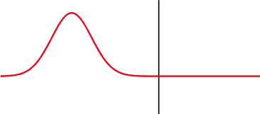
Signal Integrity (SI) means the signals created at the transmitting or driving end of a circuit reach the receiving end intact enough to be used. Ideally, signals would not change on their way to the receiver because as the frequency and density of circuits increase, signals degrade, and SI becomes an issue.
Factors that Affect Signal Integrity (SI)
There are several factors that affect SI. They become more prevalent with higher frequencies and higher component densities. Here are a few common factors to pay attention to:
Route Length
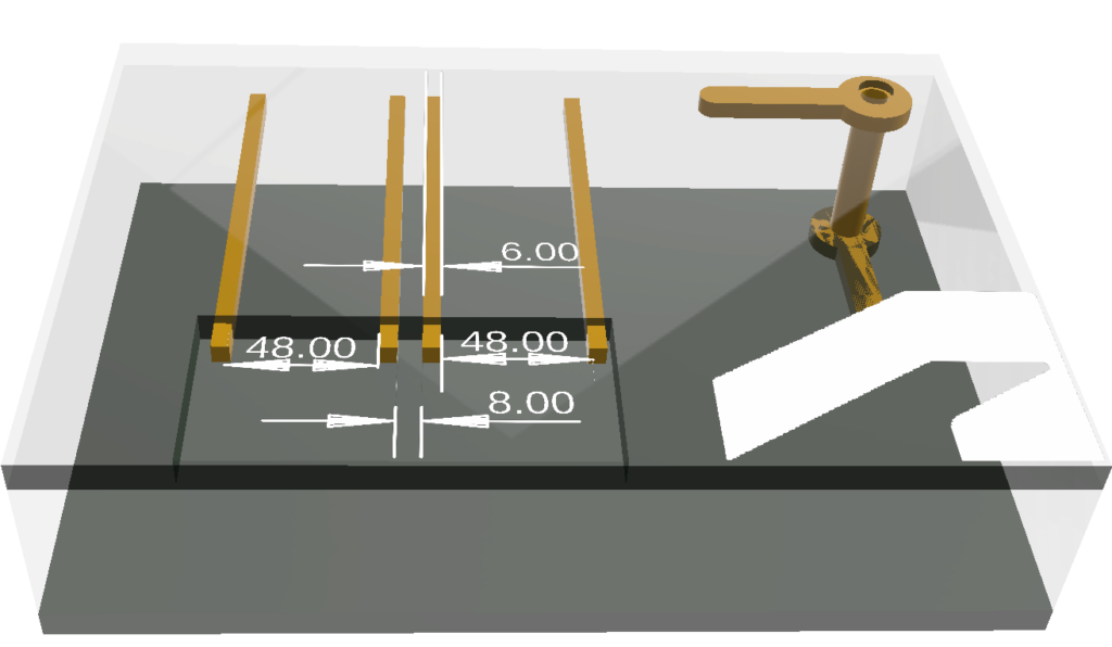
At higher frequencies, the time it takes a signal to travel from the transmitting driver to receiving device matters. This is especially true for differential communications. Pulse travel time along a trace is proportional to its length. Meandering ensures that trace lengths are equal. High-speed differential lines also need to have equal electrical lengths.
Clock Skewing
One consequence of uneven route lengths is clock skewing, a situation where clock edges arrive at times significantly later than the data they are clocking. Consumer products that use memory and sensor modules commonly have high-speed SPI and I2C clocks and data. In this case, you must ensure that data paths and clock paths to all ICs remain constant and within specifications.
Impedance Matching
Unmatched PCB transmission lines, which are what microstrip and striplines are, will degrade your signals. Lines need to match up to the driving circuit impedance for maximum power transfer. Common PCB microstrip and stripline impedances are around 100 Ω. Most radio frequency circuits and antenna feeds use 50 Ω. Termination resistors, which match the impedance of the line, sit at the end of a transmission line.
Pulses reflect back to the driver if the end impedance doesn’t match or gets terminated. This would degrade your signals.
Changes in impedance along lines also result in reflections and signal degradation. Keep high-speed differential line spacing constant.
PCB manufacturers will create test “coupons” of your PCB and Time Domain Reflectometry (TDR). Tests verify that you’ll achieve the impedances you want using the dielectric of the substrate(s) you use. Work closely with your CM / PCB manufacturer to ensure they produce the boards with the impedances you need.
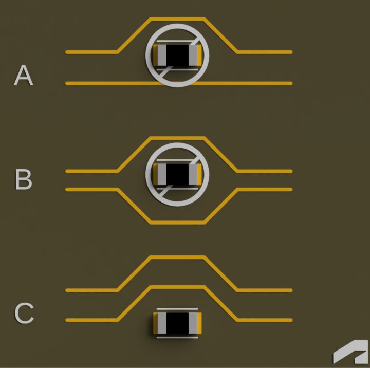
Stubs
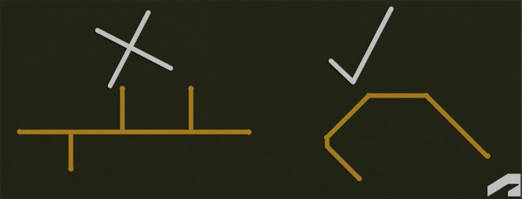
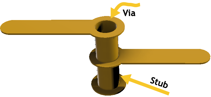
Stubs form a small transmission line, and they too can cause reflections. Try to run high-speed signals via continuous routes to minimize reflections. Stubs appear from vias that have traces that do not connect the topmost and bottom-most layers.
They begin to matter when the frequency wavelengths begin to approach ¼ wavelength. But remember: you need to consider the rise time of signals to determine the highest frequencies to consider. Not the base frequency of the signal. In extremely high-speed cases, via stubs may need back-drilling of vias to remove stubs.
Crosstalk
During the early days of telephony, people noticed that when multiple phone conversations took place in bundled wire cables, people could hear other people’s conversations. This type of signal coupling is called crosstalk. The term has stuck around. It now means any signal injected from adjacent wires.
On two-layer boards, an easy way to reduce or eliminate crosstalk is to route signals at right angles to each other on the top and bottom layers. Keeping adjacent parallel signals well separated is another common technique that reduces crosstalk. A good rule of thumb is to keep differential pairs 8W away from other signals, where W = width of trace, and 50 mils away from clock traces.
Using a ground plane will keep electric fields from spreading out too far and interfering with adjacent traces.
Increase High-Speed PCB Performance
Maintaining good signal integrity in high-speed layouts is challenging. Follow the guidance above to greatly increase your signal quality and PCB performance. View the rest of the series here:
- High-Speed PCB Design Part 1: How To Identify a High Speed Design
- High-Speed PCB Design Part 2: What to Consider First
Ready to get started with high-speed PCB design? Try the Fuson 360 Signal Integrity Extension today.