PCB DESIGN WITH AUTODESK FUSION

The ultimate PCB design software

Autodesk Fusion designs, simulates, and manufactures high-quality PCBs seamlessly. Discover the power of PCB design software that integrates mechanical and electronic design.

pcb-design

About PCB design

Printed circuit board (PCB) design is the process of bringing electronic circuit boards to life.

Printed circuit boards (PCBs) are used in many  electronic devices—from small consumer products to large industrial machines.

Excellent PCB design creates functional, reliable, cost-effective circuit boards that meet the electrical and physical requirements of the devices they will be used in. PCB design is also critical to make sure devices function properly and minimize the risks of electrical shorts, interference, and other problems that can arise with poorly designed circuits.

pcb-design-software-fusion-360

About PCB design software

PCB design software designs and creates printed circuit boards (PCBs). PCB design software creates circuit board designs and places components and routing connections between them.

Software for PCB designing can also be used to make sure that the layout meets design requirements, including trace width and clearance between components.

Benefits of PCB design software

Improved accuracy

Make sure that circuit boards are designed with a high level of accuracy. Reduce the risk of errors and improve product reliability with electronics simulation.

Increased flexibility

Eliminate the need for physical prototypes, reducing costs and design iterations by easily modifying the design directly in the software. 

Better collaboration

Multiple designers and cross-functional teams can work on a design concurrently reducing design time and improving product quality.

Time and cost savings

Features such as interactive routing, schematic capture, and component libraries reduce design time. PCB design software also reduces the cost of production by optimizing the placement of components, reducing the circuit board size, and more.

Consumer product design using Autodesk Fusion PCB design software

PCB design for consumer products

Product designers require solutions that help them bring consumer products to market faster and to easily transition from design to production.  Autodesk Fusion enables seamless integration of 3D design and PCB design.

  • Iterate faster with simultaneous collaboration capabilities
  • Minimize delays with ECAD/MCAD integration
  • Simplify project communications with connected teams in one platform

PCB design process

electronic-component-pcb-design

Electronic component placement

The PCB design process begins by converting an electronics schematic diagram into a physical circuit board layout. Then it’s time to put your problem solving skills to the test by placing electrical components within a tightly constrained space.

pcb-routing

PCB routing

The PCB routing process is both an art and a science. Using physical wires, you’ll define electrical connectivity between components on a PCB layout. No two circuit boards are the same, the routing is what makes your design unique.

ecad-mcad-integration

ECAD-MCAD integration

Nearly every PCB design exists within a mechanical product. Using Autodesk Fusion native ECAD & MCAD makes it easy for electronics and mechanical engineers to concurrently work on the same design to validate product fit, form, and function.

pcb-design-fusion-360

How to design a PCB board with Autodesk Fusion

To create a PCB in Autodesk Fusion electronics, launch the software and open the electronic design module from the file drop-down menu. Here, you'll find all the necessary tools for designing your schematic and board layout professionally. You can begin by creating a schematic and use the extensive library of components to add the required parts to your design. Autodesk Fusion electronics enables easy component placement and connectivity, for a streamlined design process.

PCB design features in Autodesk Fusion

Constraint manager in Autodesk Fusion

Design constraint manager

Uncover meticulous design guidelines, guaranteeing scalability and organization for the most intricate PCB design constraint manager. Autodesk Fusion provides high-quality, error-free production through strict compliance with industry standards and optimization of design specifications.

Schematic design in Autodesk Fusion

PCB and schematic design synchronization

Fusion's PCB and schematic design synchronization ensures confidence and minimizes the risk of errors, enhancing the reliability of the final product. This integrated approach streamlines the design process, reducing the likelihood of discrepancies and ensuring consistent performance.

SPICE simulation in Autodesk Fusion

SPICE simulation

Verify that your design parameters are correct with our easy-to-use SPICE simulation tool, available in Fusion Electronics. Our repository of components makes it easy to get you started or build your own. It is SPICE compatible.

PCB design collaboration in Autodesk Fusion

Cloud collaboration

The Fusion electronics design capabilities provide managed team access to the project with instant updates to the latest version. Built-in versioning, milestone referencing, and web-based access to designs enable stakeholders to comment, track progress, and collaborate effectively.

ecad-mcad-electrical-mechanical-design

PCB design: Where mechanical meets electrical design

Intelligent products require integrated electrical and mechanical characteristics. Learn how to seamlessly share design changes and collaborate between mechanical and electrical workflows in Autodesk Fusion.

PCB design basics

Get started with PCB design software with these tutorials, articles, and tips.

pcb-design

What's a PCB?

Learn about the construction of a PCB (printed circuit board) and how they fit into today’s world of advanced electronic devices.


pcb-design-basics

PCB layout basics

Learn how to convert a circuitry schematic design to a PCB layout and begin placing your electronic components.


pcb-manufacturing

PCB manufacturing

Learn how to produce manufacturing data for a printed circuit board using the CAM processor in the PCB editor.


Schematic capture

Schematic capture

Schematic capture is what you do when you take a PCB design from your head or from scribble notes and turn into a schematic diagram using PCB designing software. It’s not simply a case of representing all the necessary parts of the circuit, the diagram must also include information on the connections between these, and these are often referred to in electronics CAD as ‘nets’. Circuit board design software such as Autodesk Fusion simplifies this process and helps you to keep track of everything.

PCB design software in 3D

PCB design software in 3D

Circuit diagrams may be two-dimensional, but circuit boards are definitely not. Autodesk Fusion allows you to preview your PCB designs in 3D from angle you choose, so you can take a look at it from a whole new perspective. This can help you to visualize more effectively how different components will interact, and how well the whole design will fit inside its casing, without the need to build expensive and time-consuming prototypes only to have to go back to the drawing board.

Review and share PCB designs

Review and share PCB designs

Effective PCB design depends not just on connecting components and circuits but on connections between minds and an approval hierarchy. With Autodesk’s PCB software, you can quickly and easily share your designs with colleagues and peers for feedback and guidance, review colleagues' work, or get inspired by others’ PCB designs. You can even work on PCB cad designs with others simultaneously, speeding up design time and allowing you to benefit from having additional brain power on the task.

PCB design resources

Learn the basics of how to work with 3D PCB design in Autodesk Fusion. Get answers to some of the most commonly asked questions from the electronics community.


Design your printed circuit board (PCB) layout with these tips for routing, component placement, heat dissipation, and more.


Moisture, humidity, dust? No problem! Here are the main considerations that you need to make when designing PCBs that will live in harsh environments. 


Learn how the Autodesk Fusion Signal Integrity Extension improves product compliance and performance, reduces costly physical PCB testing and prototyping, and accelerates high-speed PCB development.


This PCB design advice that will help you lower costs, have fewer production failures, and improve product quality.


PCB design revisions used to be costly and time-consuming. Not anymore! Here’s why PCB designers need 3D modeling software.


PCB design software FAQs

What is a PCB layout?

A PCB layout refers to the physical design or arrangement of electronic components and their interconnections on a printed circuit board (PCB). PCB layout is a critical step in the design of electronic circuits, as it directly impacts the performance, reliability, and cost of the final product.

How do I choose the right PCB design software?

Factors to consider when choosing PCB design software includes:

  • Functionality
  • Ease of use
  • Compatibility
  • Cost
  • Community and learning resources.

Autodesk Fusion is an affordable fully integrated electronics design and manufacturing software.

Can I collaborate with others using PCB design software?

Yes, Autodesk Fusion offers collaboration features that allow multiple users to work on the same design simultaneously. They can share design files, and communicate in the same software environment in real-time. Collaboration features include version control, commenting, and real-time collaboration.

Can I simulate my PCB design before production?

Yes, PCB simulation software, like Autodesk Fusion allows you to test and validate the functionality and performance of your design without having to physically build and test a prototype.

What file formats are used for PCB design?

File formats for PCB design include, Gerber, ODB++, dwg, pick and place file, BOM, dxf, nc drill file, IPC netlist, Sch and PCB files, SPICE models, IBIS, and BSDL.

Can I import my existing schematics and designs into a new PCB design software?

If your schematics are made with EAGLE all you have to do is to open them in Fusion electronics, there is no import process needed. Create a project folder and upload them.

Where can I find PCB component libraries?

You can find a wide array of free and open-source component libraries in Autodesk’s Eagle online libraries. There you’ll find component models that you can use in your PCB design CAD software, from microcontrollers and USB connectors to stepper motor drivers, semi-conductors and terminal blocks. This means that you don’t have to spend time inputting the component designs yourself, so you can focus on the more important tasks of printed circuit board design.

What is a PCB?

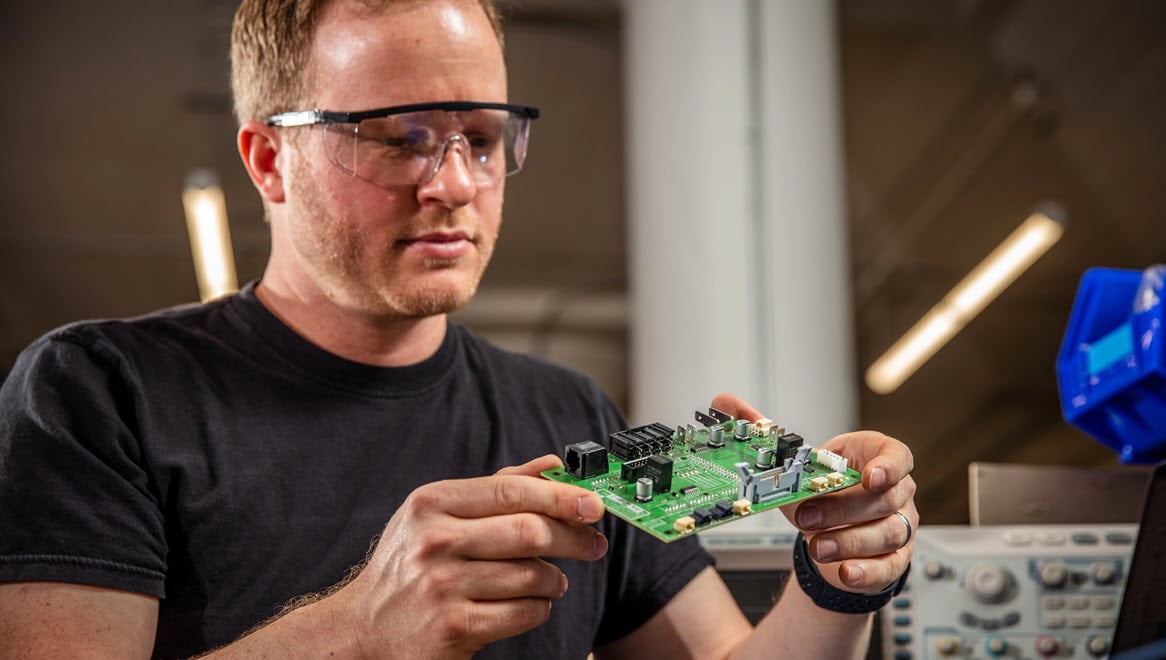
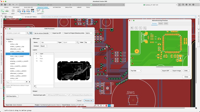
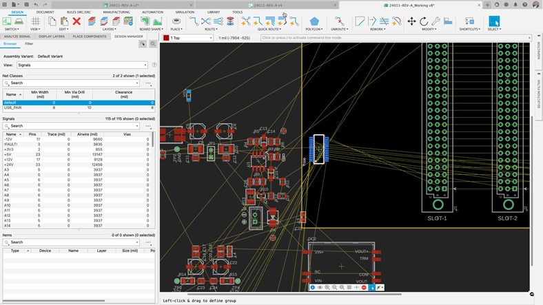
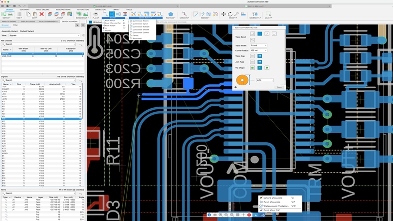
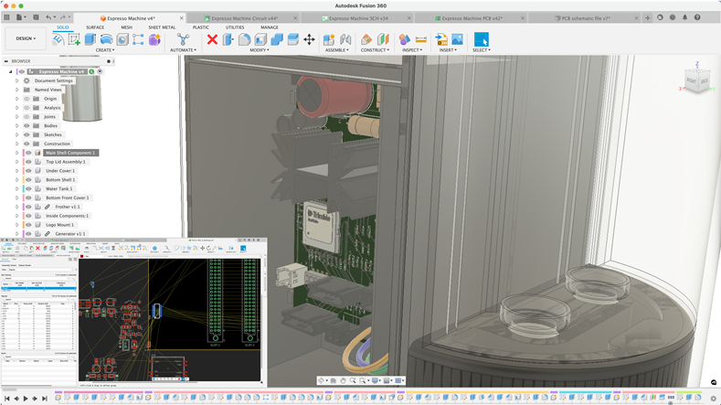
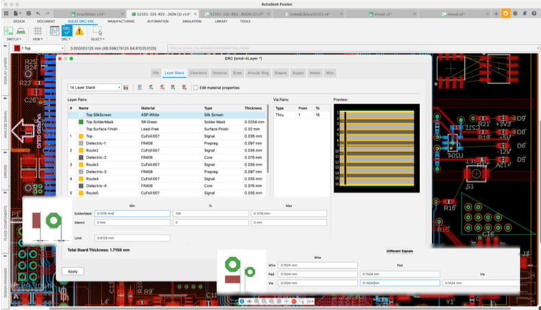
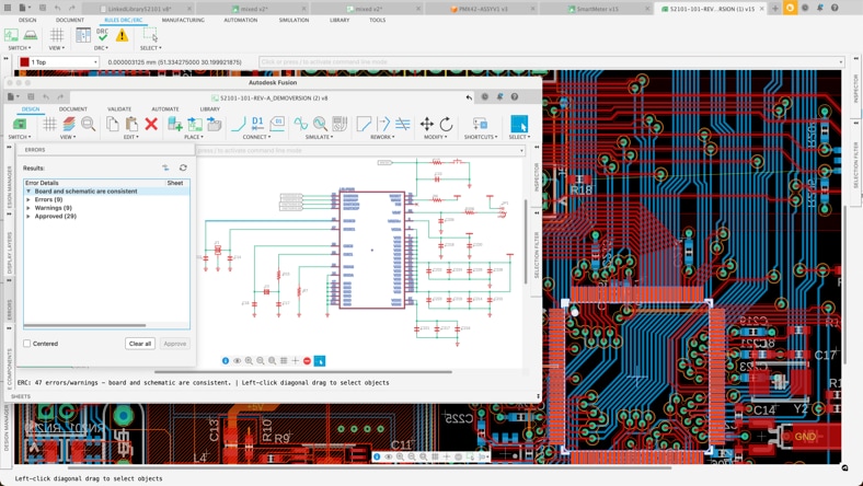
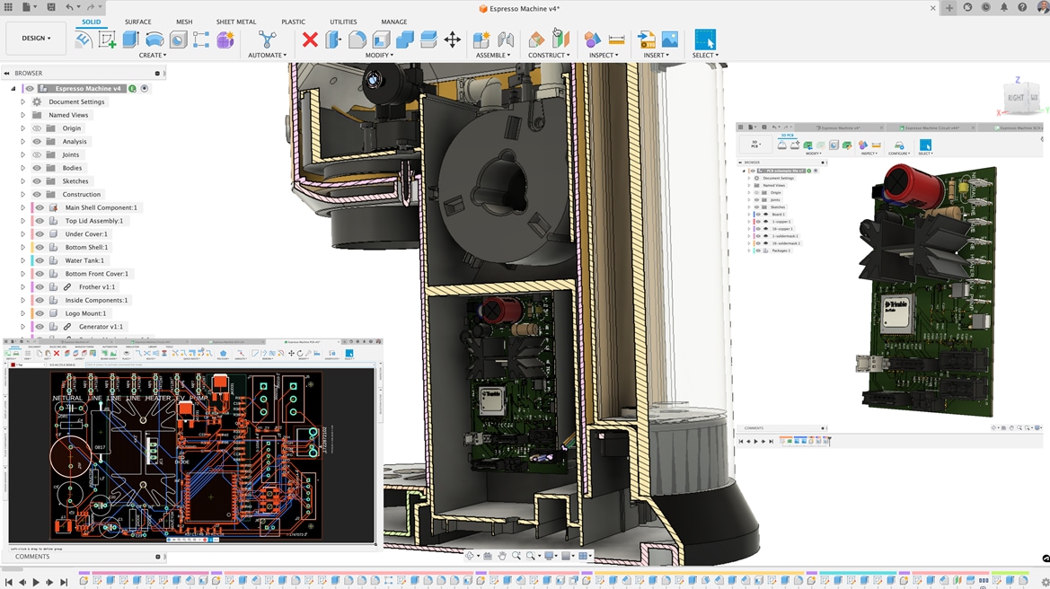
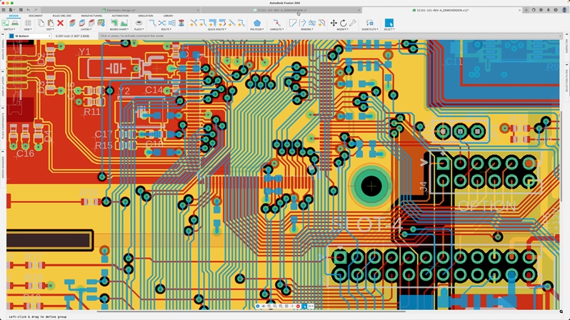
A Printed Circuit Board (PCB) is a board used to mechanically support and electrically connect electronic components using conductive pathways, traces or tracks which are etched from copper sheets laminated onto a non-conductive substrate.


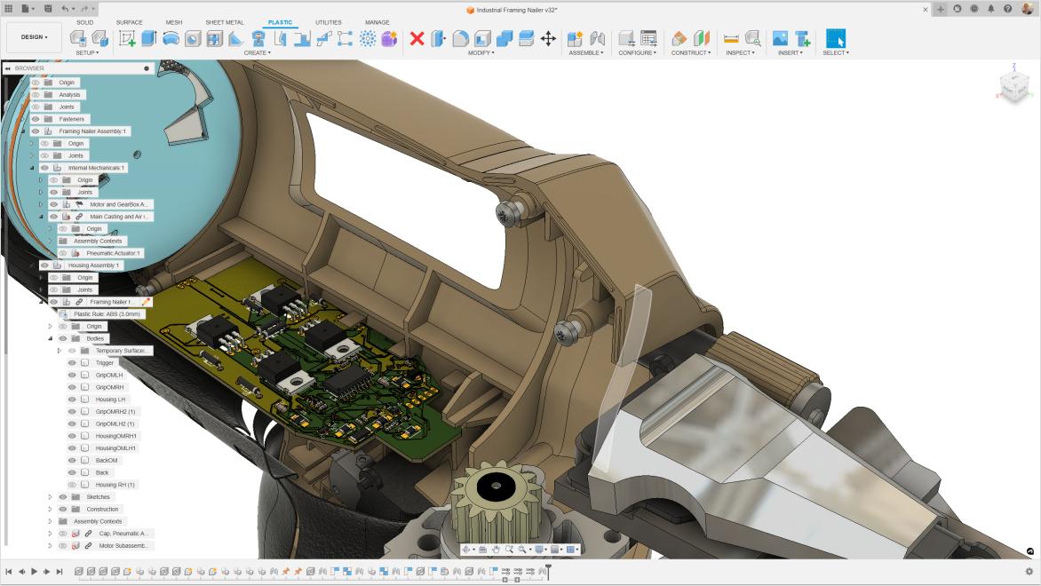
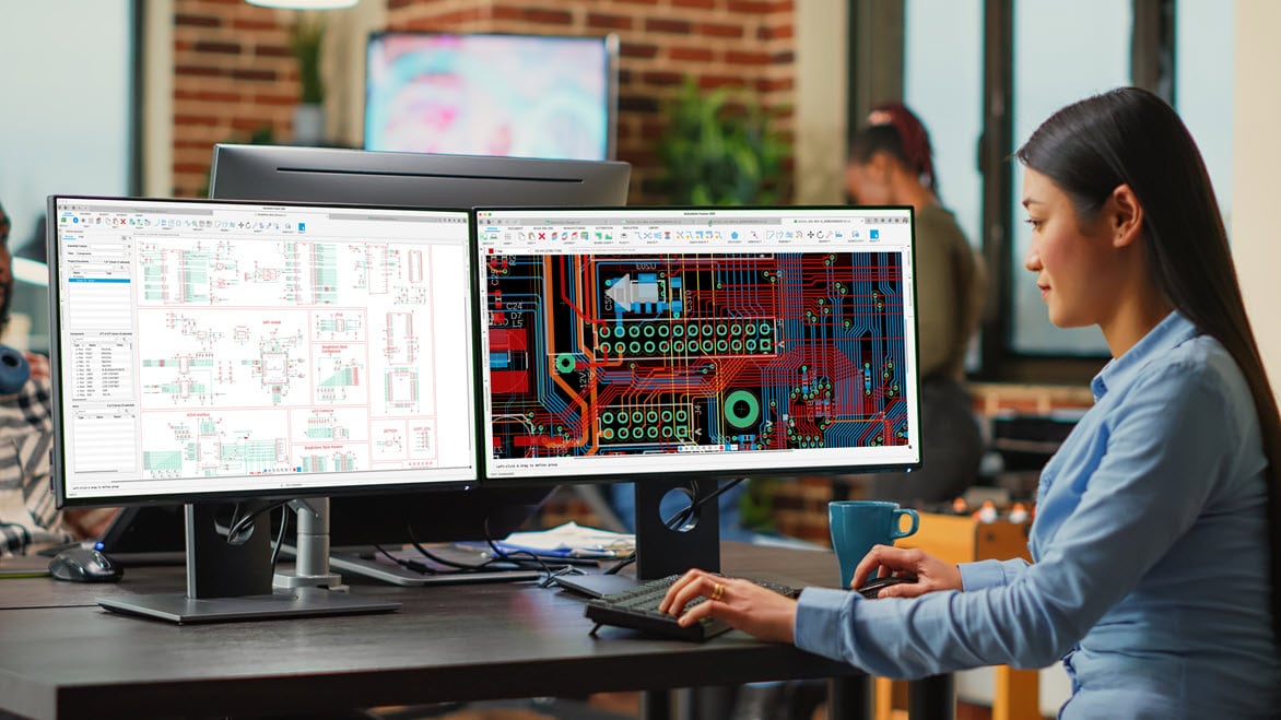
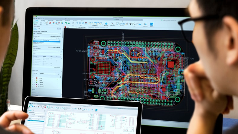
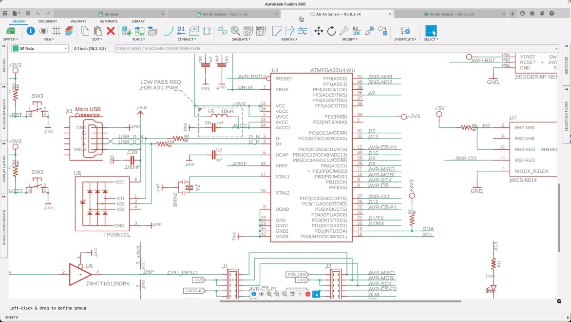
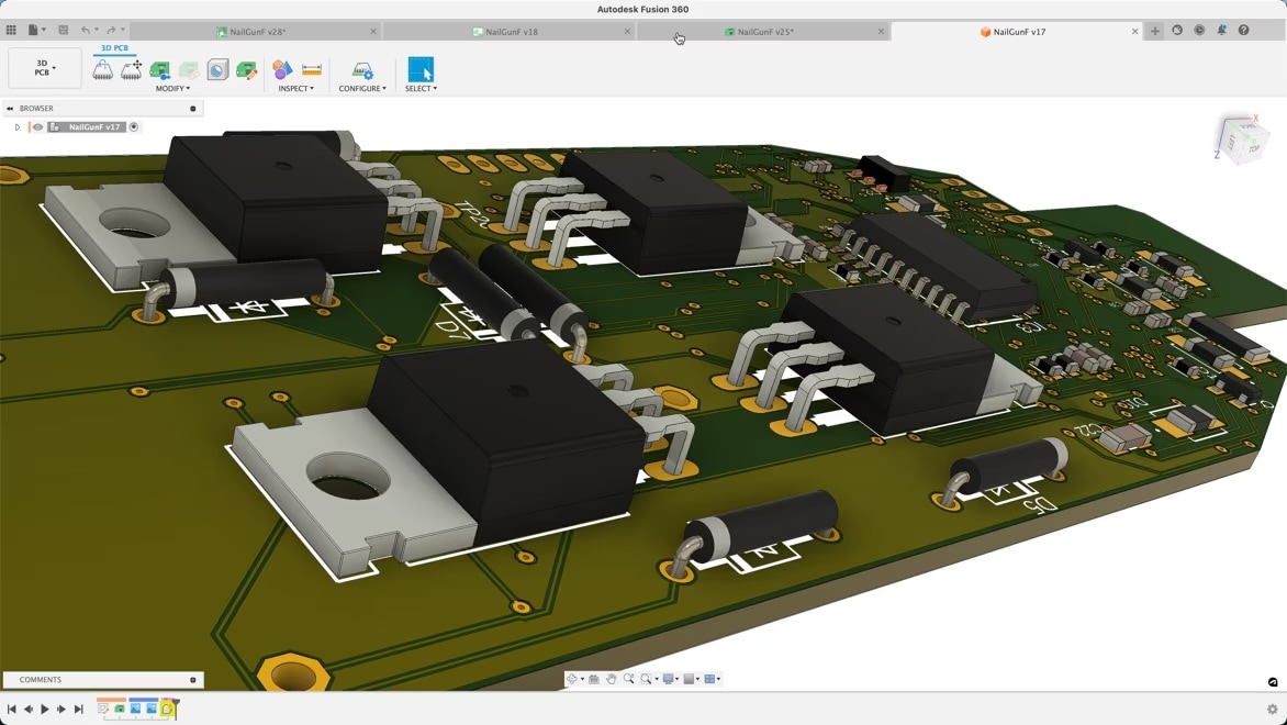
PCBs are used in virtually all electronic devices. They provide a solid surface for mounting components and establish the necessary electrical connections between them. The layout and physical design of a PCB play a critical role in determining how the device functions.

What are the types of PCBs?

The three most basic types of Printed Circuit Boards (PCBs) are:

  1. Single-Sided PCBs: These are simple and most common types of PCBs. They contain only one layer of substrate or base material, which is coated with a thin layer of metal, typically copper due to its excellent electrical conductivity. The metal layer is then coated with a protective solder mask and silk-screen to print details.
  2. Double-Sided PCBs: As the name implies, double-sided PCBs have two coated sides of material with metal. Holes in the board allow circuits on one side to connect to circuits on the other.
  3. Multi-Layer PCBs: These are more complex, consisting of several layers of substrate material that are glued together with layers of insulating material between each one. Multi-layer PCBs can have anywhere from 4 to 12 layers, though some complex PCBs can have over 42 layers. These extra layers can be used for additional power supply layers, ground planes, and for additional circuitry.
See more FAQ